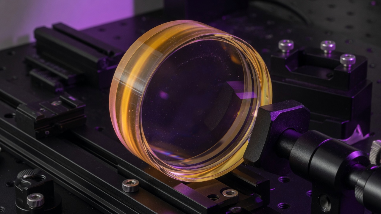
A CO₂ OEM rarely fails the blank. They fail the coating callout. Zinc selenide at 10.6 µm has refractive index n ≈ 2.403. From the Fresnel equation for normal incidence, (n−1)²/(n+1)², each uncoated air–ZnSe interface reflects ≈ 17 %. Two surfaces, incoherent addition, and you have already dumped a third of the beam before bulk absorption is even in the model. That energy does not disappear: it becomes a standing wave in the cavity, a ghost on the workpiece, or heat in the mount.
Optical thickness, not “paint it AR”
A single-layer quarter-wave AR is the industrial default at one design wavelength. Optical thickness nd = λ/4 at 10.6 µm means a physical thickness of about 1.3 µm if the film index is ~2.0, or ~2.6 µm if you are using a lower-index fluoride. That is not a visible-band coating scaled up. Layer thickness control, rate stability and stress are a different process window from a 550 nm V-coat.
Multilayer stacks (typically a low/high pair or a three-layer QWOT design) push residual reflectance below 0.5 % per surface over a useful angular cone. Dual-band designs — 10.6 µm plus a visible alignment channel around 633 nm or 650 nm — are what let an assembler see the beam without a separate HeNe window. Dual-band is not free: you trade some residual R at 10.6 µm and you introduce more interfaces that can absorb.
Absorption is the real LIDT limiter
Laser-induced damage at 10.6 µm CW is almost never a dielectric avalanche the way 355 nm is. It is thermal. Coating absorption of 0.2 % on a 2 kW, 8 mm 1/e² beam is 4 W dumped into a few square millimetres of film and the first microns of ZnSe. With ZnSe thermal conductivity around 18 W·m⁻¹·K⁻¹, that is enough to run a thermal lens and, if the film is stressed or contaminated, a pit.
Historic ThF₄ layers had excellent index contrast at 10.6 µm and are largely gone from Western process books for environmental and regulatory reasons. Modern stacks use ZnS, YbF₃, YF₃ and similar IR dielectrics. Ask the coater for:
- Residual R per surface at 10.6 µm, AOI 0° and at your working AOI (often 5–15° on a fold).
- Absorption of the coated witness, not just the uncoated substrate calorimetry.
- LIDT in kW/cm², CW, 10.6 µm, with beam diameter and test duration stated. “15–25 kW/cm²” without a diameter is not a spec.
- Environmental: humidity, salt fog if the head lives on a shop floor, and whether the outer layer is a moisture barrier.
What to put on the print
Write “AR both sides, R < 0.5 %/surface at 10.6 µm, AOI 0–10°, absorption < 0.2 %” if that is what you need — then fund the witness. If you also need a visible channel, specify the alignment wavelength and a maximum R or a minimum T there, and accept that 10.6 µm residual will move. Do not specify a 400–700 nm broadband AR on ZnSe and expect 10.6 µm to come along for the ride.
InfraSpec Optics coats ZnSe, ZnS and Ge for 10.6 µm OEM programs and returns the T/R trace with the parts. Use the coating page for stack families, then send the print.
References. Connolly et al., Proc. SPIE 181, 141 (1979) and Crystran (n = 2.4028; 29.1 % two-surface loss at 10.6 µm). Hellma / Crystran (k ≈ 18 W m−1 K−1; dn/dT +61×10−6 K−1). Zi, X. et al., Coatings 15, 536 (2025) — ZnS/YbF3 AR on CVD ZnSe, CW LIDT 11,890 W/cm² at 1.5 mm, 60 s.