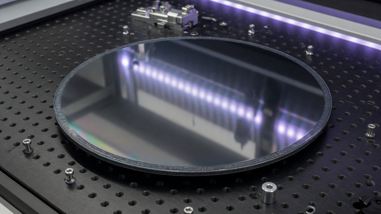
Crystalline silicon is opaque in the visible. The indirect gap is 1.12 eV at 300 K, so the crystal starts to transmit past about 1.1–1.2 µm. Useful window material through SWIR and into MWIR, depending on thickness, resistivity and coating. For 1.55 µm laser windows and many SWIR sensors it is the economical, scalable answer. Harris (SPIE, 1999) and every IR handbook put it on the MWIR list, not the 10.6 µm list.
Strengths
Wafer infrastructure, large diameters, Knoop far above ZnSe, high index (n ≈ 3.42 at 3 µm class — check the lot table). Thinner elements for a given optical power, with the usual AR burden: one uncoated face is already ~30 % reflection. For 1.5 µm-class laser and SWIR imaging windows, Si is first on the shortlist.
Phonons close the LWIR
Do not replace Ge with Si on an 8–12 µm imager. Multiphonon absorption kills transmission in typical window thicknesses long before 10.6 µm. A CO2 focusing lens in silicon is the wrong crystal. Multi-spectral systems that need true LWIR plus NIR become two materials (Si + Ge, or ZnS/ZnSe), not one Si optic. High-resistivity float-zone Si is a THz / FIR special, not an LWIR camera window — different RFQ.
Resistivity is a spec
Free-carrier absorption tracks doping. “Optical grade silicon” on a PO without resistivity is how a 1.55 µm window comes in absorbing. AR for 1.5–5 µm is not a telecom V-coat. Match the stack to the sensor or the laser line. Explore cut-on in the Spectral Explorer (Si is gone by 10.6 µm), then the quote form.
References. Harris, D.C., Materials for Infrared Windows and Domes, SPIE (1999). Crystran / handbook Si transmission (cut-on ~1.2 µm; LWIR closed in typical thickness). Palik, Handbook of Optical Constants of Solids (Si n, k). TYDEX high-resistivity FZ-Si for THz — different product.