When an OEM asks for “a ZnSe window for 10.6 µm,” they are asking three things: bulk absorption, CVD grade, and whether the AR stack survives the fluence. Connolly, diBenedetto and Donadio published the CVD index everyone copies — n = 2.4028 at 10.6 µm (Proc. SPIE 181, 141, 1979; Tatian fit, Appl. Opt. 23, 4477, 1984). Crystran lists the same number and 29.1 % two-surface Fresnel loss. Laser-grade bulk absorption is ~5×10⁻⁴ cm−1 (Hellma 5.0×10⁻⁴; Coherent < 0.0005; Raytheon ADA042147 already had 4×10⁻⁴ in 1977).
Grade is not marketing
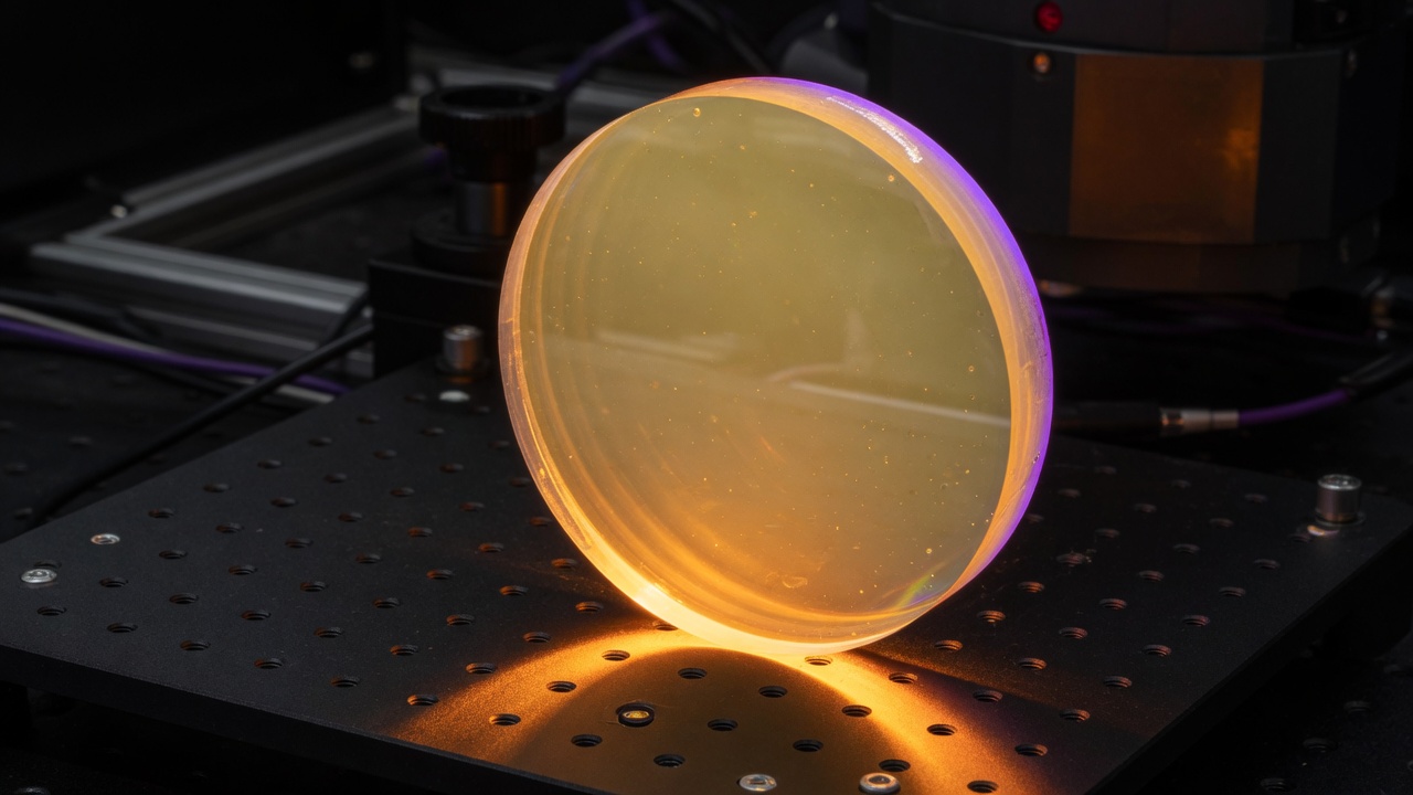
Scatter centres become damage initiators. Grain on commercial CVD is typically < 100 µm (Coherent; Raytheon table ~70 µm). Surface quality 40-20 typical, 20-10 on request. Figure λ/4 class at the test wavelength, which must be named — see the λ/10 note. Knoop 105–120. Gloves. The crystal is yellow because the gap is about 2.70 eV at room temperature; a HeNe at 633 nm still goes through. Germanium does not.
Coatings decide the resonator
One uncoated face returns ~17 %. Dual-side AR at 10.6 µm is the industrial default. Dual-band 10.6 µm + 633 nm keeps alignment and gives back a little at the laser line. Zi et al., Coatings 15, 536 (2025), measured a ZnS/YbF3 10.6 µm AR on CVD ZnSe at 11,890 W/cm² CW LIDT (1.5 mm spot, 60 s). Witness samples from the same run as the lot. A spectrophotometer trace of a previous lot is not a qualification.
Do not swap ZnS to save cost on a kW head
ZnS is harder and better in rain (Harris, SPIE 1999, ch. 6). Absorption at 10.6 µm is usually worse than laser-grade ZnSe. Thermal lensing: dn/dT ≈ +61×10−6 K−1, k ≈ 18 W m−1 K−1. Send power, 1/e² diameter, CW vs pulsed, environment, and whether the part is a focusing lens, meniscus or flat. Use the Spectral Explorer, then the quote form.
References. Connolly et al., Proc. SPIE 181, 141 (1979). Tatian, Appl. Opt. 23, 4477 (1984). Miles et al., DTIC ADA042147 (1977). Hellma CVD Zinc Selenide®. Crystran ZnSe. Harris, D.C., SPIE (1999). Zi et al., Coatings 15, 536 (2025).